*Experienced design team
95% engineers with electronic engineering Bachelor degree; Over 5 years design experience.
*Advanced design capability
Up to 40 layers, maximum PINs 60000
*Flexible for customers' requirements
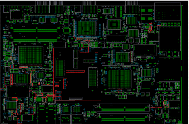

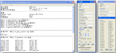
Support Mainstream Design Tools in the Industry : Allegro ,Pads, Mentor Expedition .
Design Type : High speed ,Analog,Analog-digital mixed , high-density ,high-voltage,high-power
RF ,back plate ,ATE,felexible board and aluminum substrate,etc.
Design Lead Time :
| The Number of Pins | Normal Finish Time (Working Day) |
|---|---|
| 0–1000 | 3–5 |
| 2000–3000 | 5–7 |
| 4000–5000 | 8–12 |
| 6000–7000 | 12–15 |
| 8000–9000 | 15–18 |
| 10000–13000 | 18–20 |
| 14000–15000 | 20–22 |
| 15000–20000 | 22–30 |
| 20000–30000 | 25–35 |
